Teltec Pacific is a technical Sales and Service organisation serving the Semiconductor, Photonics and Optoelectronics Industries in Asia Pacific countries.
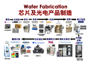
Wafer Fabrication
Kayaku Advanced Materials develops, manufactures, sells, and supports specialty niche chemicals for semiconductor/IC, thin film head, and other electronic manufacturing applications. The primary focus is photosensitive materials, such as photoresists, and other ancillary products. Kayaku Advanced Materials consists of proprietary and non-proprietary products requiring state-of-the-art technical expertise, high reproducibility, high product cleanliness, and specialty microfiltration.
Kayaku Advanced Materials manufactures all of their products in their newly re-fitted 25,000 square foot facility in Newton, Massachusetts. All the products are made in environmentally controlled areas and packaged in Class 100 Cleanroom environments.
Kayaku Advanced Materials resist products are available in 500ml, 1 Liter, 4 Liter Amber glass bottles, in addition we can package into 10 and 20 Liter Nowpaks. The ancillary products are available in 4 Liter Polyethylene bottles, Nowpaks and 55 Gallon drums.
LightLink Optical Waveguide Materials (NEW product !)
SU-8 2000 & 3000 Series Resists
The SU-8 product line consists of chemically amplified; epoxy based negative resists with high functionality, high optical transparency and are sensitive to near UV radiation. Cured films or topography are highly resistant to solvents, acids and bases and have excellent thermal stability, making it well suited for permanent use applications.
SU-8 2000 Permanent Epoxy Resists
SU-8 2000 chemically amplified, i-line resists are well-suited for the fabrication of permanent device structures. These negative tone, epoxy based resists exhibit excellent chemical resistance and low Young's Modulus which makes them ideal for fabricating micro/nano structures such as cantilevers, membranes, and microchannels.
Material uses:
Fabrication of PDMS molds
Structural components such as micro arrays, fluidic channels, display pixel walls and dielectric layers
N Chronis, LP Lee, UC Berkeley, μTAS 2002, 754 (20
Passivation layer for diodes.
Encapsulation with imaged vias.
LED Passivation Application
SU-8 3000
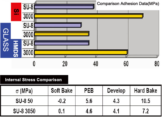
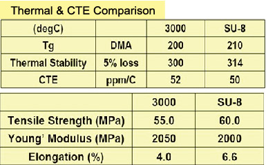
SU-8 3000 has been formulated for improved adhesion and reduced coating stress. It is being used where high bond strength and improved flexibility for microstructure fabrication is desired. As a result, adhesion to the substrate is greatly improved.
Material uses:
Waveguides
Microfluidics
Stamps
Material attributes:
Improved adhesion
Reduced coating stress
Vertical sidewalls
Greater than 100 μm film thickness in a single coat
Excellent dry etch resistance
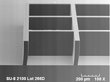
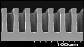
10µm features in 50µm SU-8 3000 (contact expose) Source: MicroChem
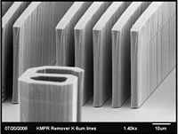
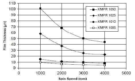
KMPR® 1000 i-line photoresist is a high contrast, epoxy based photoresist that can be developed in a conventional aqueous alkaline developer (TMAH) and stripped from the substrate using Remover PG or plasma. KMPR is designed to coat 4-110 µm in a single step using four standard viscosities.
Lithography can be used to form KMPR molds that have the required dimensional accuracy and sidewall verticality for micro electroforming.
Deep reactive ion etching (DRIE), KMPR will survive dry etch for the extended periods of time necessary to perform >20 µm deep etching with HAR.
Material uses:
MEMS
DRIE
Electroplating
Permanent Structures
Material attributes:
High aspect ratio with vertical sidewalls
High chemical and plasma resistance
Greater than 100 µm film thickness in a single coat
Excellent adhesion to metals
Excellent dry etch resistance
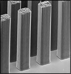
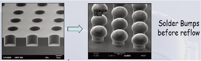
Plating
Permanent
Deep Etch
Plating (100 µM tall Ni posts, KMPR removed)
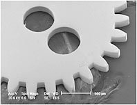
Electroformed Ni gear after stripping KMPR Source: Univ. of Birmingham
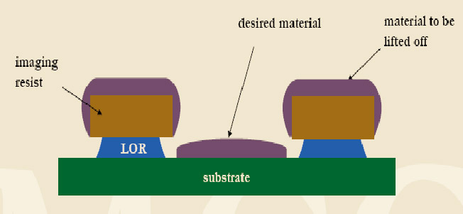
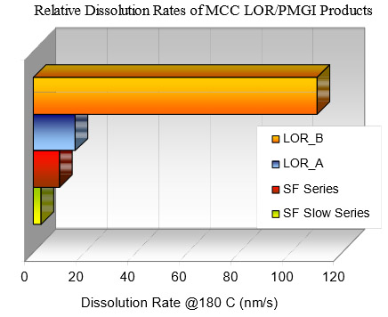
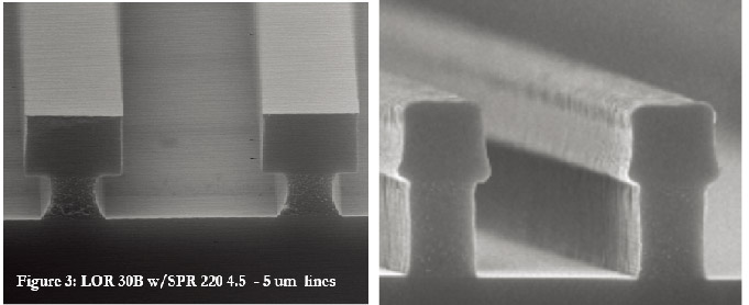
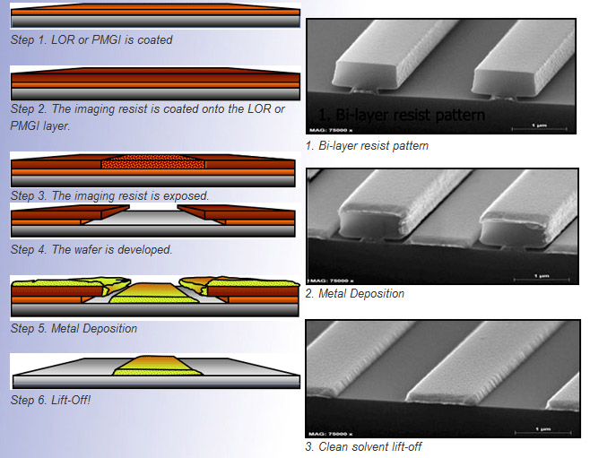
PMGI and LOR resists enable high yield, metal lift-off processing in a variety of applications from data storage and power devices, to BAW filters. Used beneath photoresists in a bi-layer stack, PMGI and LOR extend the limits of lift-off processing beyond where single layer resist strategies can reach. This includes very high resolution metallization (0.25 microns) to thick (4µm) metallization. These unique materials are available in a variety of formularies to meet virtually any customer need.
Material uses:
Metal lift-off processing
Airbridge fabrication
Release layers
Material attributes:
Won’t intermix when over-coated with imaging resists
Single step development of bi-layer stack in TMAH, or KOH developers
High thermal stability: TG ~190 C
Removes quickly and cleanly in conventional resist strippers
Enables sub .250µm micron bi-layer resist imaging
Enables high yield, very thick (>3µm) metal lift-off processing
LOR Bi-layer Lift-off Resists
High aspect ratio with vertical sidewallsresolution, for feature size <0.25µm metallization lift-off
Undercut controllable
Good adhesion on Si, NiFe, GaAs, InP and III-V compounds etc.
High thermal stability
Remove easily and high lift off yield
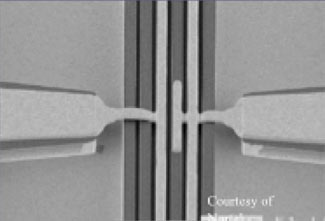
Bi-Layer Lift-Off Process Lift-Off: An enabling, additive lithographic process.
GaAs Modulator with Al airbridge Source: Nortel
PMGI used as a sacrificial layer on which the airbridge was built. The PMGI layer was subsequently removed with conventional resist removal processing.
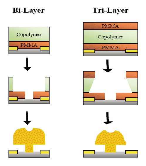
PMMA positive resists are based on special grades of polymethyl methacrylate designed to provide high contrast, high resolution for e-beam and X-ray lithographic processes. In addition, PMMA is often used as a protective layer in III-V device wafer thinning applications. Standard products include 495,000 and 950,000 molecular weights (MW) in a wide range of film thicknesses formulated in chlorobenzene, or the safer solvent anisole. In addition 50,000, 100,000, and 200,000 are available upon request.
Copolymer resists are based on a mixture of PMMA and ~8.5% methacrylic acid. Copolymer MMA (8.5) MAA is commonly used in combination with PMMA in bi-layer lift-off resist processes where independent control of CD size and shape of each resist layer is required. Standard copolymer resists are formulated in the safer solvent ethyl lactate and are available in a wide range of film thicknesses.
Applications for PMMA & copolymer resists (MMA (8.5)MAA)
T-gate resulting from PMMA/Copolymer bilayer resist stack.
Product Attributes
Feature size : less than 0.1µm imaging
E-beam and X-ray exposure
Molecular Weights (MW) : 495K, 950K, custom MW available
Solids content 2% - 11%, customized available
Molecular Solvent : Chlorobenzene (C) or Anisole (A)
Applications : E-beam usage, wafers, thinning, T-gate, etc.
Top Layer Construction Combined Layer Construction
LightLink Optical Waveguide Materials Licensed from the Dow Chemical Company.
The LightLink product line consists of materials designed and developed for the fabrication of planar polymeric optical interconnects on rigid and flexible substrates. These siloxane-based materials exhibit high optical clarity and excellent resistance to heat and humidity, making them well suited for optical waveguide applications. These materials may also be applicable to other potential applications where superior optical properties and high environmental stability are required.
Product Uses:
Multimode waveguides (830-860nm)
Single-mode waveguides (1300-1500nm, short paths)
Board-level optical interconnects
Material Attributes:
Processable using conventional manufacturing equipment and methods
Photo-definable to 10痠 at 1:1 aspect ratio using aqueous developer
High transparency in the visible and near infrared
Low optical loss of 0.05 dB/cm at 850 nm
Low birefringence of <0.0001 at 850 nm
Excellent reliability in extreme temperature and high humidity environments
High mechanical robustness
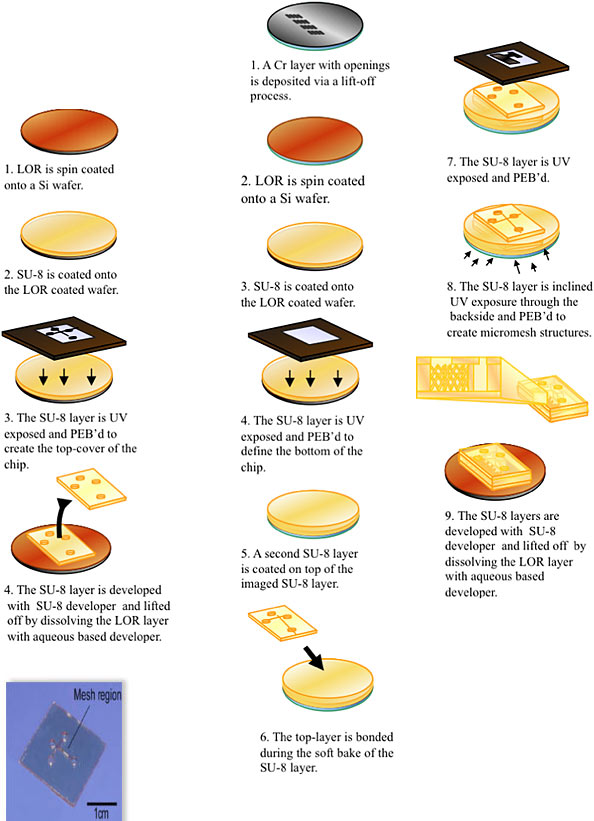
Waveguide fabrication process overview
Step 1. Coat and cure LIGHTLINK Clad
Step 2. Coat and softbake LIGHTLINK Core
Step 3. Expose, post-exposure bake and develop LIGHTLINK Core
Step 4. Coat and cure LIGHTLINK Clad
Core structure on Silicon spin-coating, softbake
and mask lithography. Source: MicroChem
Waveguide structure on FR4 PCB spin-coating,
softbake and mask lithography. Source: MicroChem
gL2000 E-beam Positive Resists
gL2000 resists from Gluon Labs are high speed, high resolution e-beam resists which offer dry etch resistance equivalent to novolac based resists. Available in three dilutions that cover a range of thickness from 200 - 1000+ nm, the resists are available in 100 ml and quart sizes. Standard and high resolution developer formulations are available in 4 liter bottles along with a specialized remover.
Film thickness: 230nm 100kV 50pA Developer: gL Developer @RT 120sec
Dot Pattern
Pitch40nm/space12.5nm
Donut Pattern
PriElex® Jettable Polymeric Materials
PriElex® is envisioned as a new suite of functional inks for inkjet printing of electronic devices. PriElex® polymeric inks are designed and optimized for jetting and are suitable for maskless lithography, rapid prototyping, and clean, non-contact printing. Material formulations are tailored for critical inkjet properties such as viscosity, evaporation rate, and surface tension, and exhibit improved latency, firing stability, and resolution over standard resist formulations.
MicroChem currently offers XP PriElex® SU-8 1.0, an inkjettable SU-8 ink, adding to the developer's toolbox of printable materials available for the fabrication of single or multi-layer structures. Ink development was performed around the FUJIFILM Dimatix DMP printer, one of the most common R&D and prototyping inkjet tools.
Other PriElex® functional inks are envisioned, with some currently under development.


.jpg)
.gif)
.gif)
.gif)
.jpg)
.jpg)
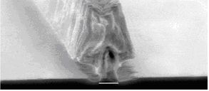 T-gate resulting from PMMA/Copolymer bilayer resist stack.
.jpg)