


|
Categories
News & Exhibitions
Applications
Video
|
PVA TePla |
||||||||||||||||||||||||||||||
|
Originating from the former TePla AG Munich, the division Plasma Systems designs, develops and builds customer specific plasma equipment. The division specializes in technologies used for the surface modification of substrates through the controlled application of plasma.
|
|
Index Chip Packaging - Bond Pad Cleaning - Plasma Cleaning prior to Flip Chip Underfill - Plasma Cleaning and Activation prior to Encapsulation
Failure Analysis - Decapsulation of Packaged Devices and Boards by Plasma Etching |
Chip Packaging
![]()
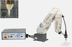
Bond Pad Cleaning

![]()
| Plasma Cleaning prior to Flip Chip Underfill
To Request Application Literature or Further Information, Click Here |
| Plasma Cleaning and Activation prior to Encapsulation
|
 Plasma cleaning in FlipChip packaging technology has become a must for yield improvement. Advanced Flip Chip devices are gaining in market prominence, and microwave plasma processes are unrivalled at penetrating the minute gaps beneath the dies. All surfaces, regardless of the volume under the die are perfectly activated and conditioned. PVA TePla’s microwave plasma consistently performs, providing void-free FlipChip underfill, optimum adhesion and a dramatically enhanced wicking speeds. Application suitability goes well beyond die sizes of 20x20mm and 50µm bumps.
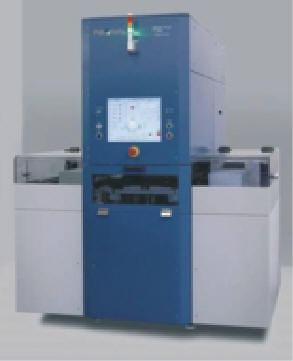
80 Plus GIGA HS: Semiconductor Innovation by PVA TePla for Microchip Packaging
Press released - (Kirchheim/Munich, October 19, 2012) The business unit Plasma Systems of PVA TePla in Kirchheim/Munich unveiled the next generation strip processing plasma system (100x300mm leadframe ready - High Speed Plasma), setting new industry standards in throughput at SEMICON Taiwan 2012.
The 80 Plus High Speed (HS) is the only single chamber system in the world featuring patent pending innovations in strip size conversion, handling and process, allowing up to three times higher units per hour (UPH) compared to other leadframe and substrate strip processing plasma systems to date. The system is targeted at high volume chip manufacturers improving yield and reliability for applications prior wire bonding, mold and flip chip underfill.
The 80 Plus High Speed is available in radio frequency (RF) and microwave (MW) technology to provide the best process solution to meet customer demands. In semiconductor microchip packaging plasma -prior wirebonding- is essential for improving the cleanliness of the bond pads. Ball shear and stitch pull strengths are dramatically enhanced by plasma cleaning. Plasma cleaning and activation is used in applications of adhesion promotion of mold compounds, eliminating yield loss due to delamination. In Flip Chip packaging technology MW plasma prior underfill has become a must for yield improvement. Advanced Flip Chip devices are gaining in market prominence, and microwave plasma processes are unrivalled at penetrating the minute gaps beneath the dies. |
|
| PVA TePla other products: |
|
|
|
|
|
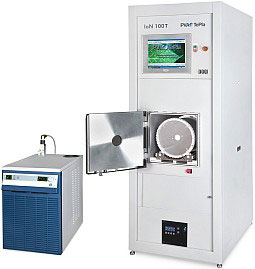
IoN Series |
GIGA 690 |
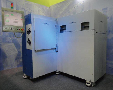
80 Plus |
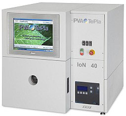
IoN SeriesThe IoN Series is designed to meet the evolving demands of our customers, emphasizing versatility and control for their surface treatment needs. Its advanced features provide state of the art process control, fail-safe system alarms and data capturing software. This enables the systems to meet stringent quality control programs in the Life Science industries. The IoN Series uses radio frequency (RF) generated plasma in a compact, fully integrated package. Another design feature of the IoN Series is the ability to quickly and easily alternate between different chamber types and electrode configurations. |
|
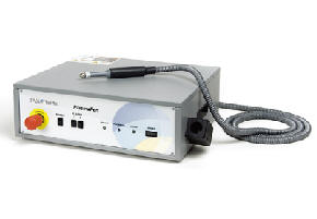
Plasma PenThe PlasmaPen™ is a patented atmospheric plasma system used to solve surface preparation problems. The PlasmaPen™ produces high density plasma with a low heating effect, giving it the ability to clean and activate the surfaces including low melting point polymers. Our worldwide customer base uses the PlasmaPen™ for a broad range of applications that span the Life Science, Electronics and Industrial markets.
The PlasmaPen™ cleans and activates the surface of materials promoting wettability of potting compounds, adhesives, inks, paints and dyes. Surface cleaning with the PlasmaPen™ ensures reliable wire and die bonding for semiconductor packaging. It has shown particular success in adhesion promotion of anisotropic conductive film (ACF) used in flat panel display manufacturing. |
|
Failure Analysis
| Decapsulation of Packaged Devices and Boards by Plasma Etching
|
(Examples of decapsulated chips) |
 Decapsulation of packaged devices (such as integrated circuits (IC’s) and printed circuit boards (PCB’s)) exposes the internal components of the package. Opening devices by decapsulation allows inspection of the die, interconnects and other features typically examined during failure analysis. Device failure analysis often relies on the selective etching of polymer encapsulants without compromising the integrity of the wire bonds and device layers. This is achieved by using microwave plasma to cleanly remove encapsulant material. The etching properties of the plasma are highly selective leaving interconnects and bond pads unaffected by the plasma etching process.
|
Related Products:
|
|
 |
IoN 10 Laboratory or pilot scale bench top microwave system ideal for resist ashing, wafer cleaning and decapsulation of electronic devices. |
| Other Applications |
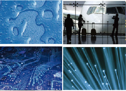
| LIFE SCIENCE
Gas plasma technology is commonly used to precision clean and activate, decontaminate surfaces, promote adhesion of functional bio-molecules and in conjunction with specific chemical vapors sterlize in-vivo and in-vitro medical devices. |
 |
| ELECTRONICS
Plasma is used in the electronics industry for a wide variety of applications ranging from adhesion promotion of encapsulants and adhesives, to enhancing the release properties of optical disc master stampers. |
 |
| INDUSTRIAL PLASMA APPLICATIONS
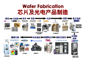
PVA TePla is a market leader in microwave plasma processing used in the fabrication of microchips, MEMS devices, photovoltaic cells, flat panel displays and detectors, and most industrial applications. • ADHESION PROMOTION |
 |