Teltec Pacific is a technical Sales and Service organisation serving the Semiconductor, Photonics and Optoelectronics Industries in Asia Pacific countries.
Bruker - AFM/Optical Profilers/FTIR
Bruker(ex-Veeco). USA
AFMs, Optical Profilers & Stylus Profilers
Bruker AXS, an operating company of Bruker Corporation (NASDAQ:BRKR) is a global market and technology leader in materials research and quality control instrumentation for elemental and crystalline structure investigations. The range of solutions covers biological crystallography and chemical crystallography, bulk material and surface sensitive X-ray diffraction, atomic force microscopy, white light optical profilers and confocal microscopes, stylus profilers, wavelength and energy dispersive X-ray fluorescence analysis, optical emission spectroscopy, and combustion analysis.
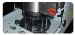
Dimension FASTSCAN - a new generation of high speed AFM imaging
Dimension FastScan™ AFM applies the performance of AFM application in polymer, semiconductor, energy, data storage and materials such as field nanoscale research. FastScan™ achieves atomic force microscopy imaging without compromising highest resolution, application flexibility, or productivity. The system delivers atomic resolution imaging while simultaneously providing real-time maps of properties derived from the individual force interactions. Whether you scan at >125Hz when surveying a sample to find the region of interest, or at time rates of 1-second per image frame in air of fluids, the Dimension FastScan redefines the AFM experience.
Dimension FastScan™ High scan rate or ultimate resolution while maintaining exceptional tip force control is a leap into a new generation of AFM use. The FastScan AFM system is the latest evolution of our industry-leading, tip-scanning AFM technology, incorporating temperature-compensating position sensors in its two scanners to render noise levels in the sub-angstrom range for the Z-axis, and angstroms in X-Y. In the air or in the liquid imaging speed is 100 times as much as the original speed, automatic laser alignment and detector adjustment, Intelligent needle inserting, shorten experiment time largely. This is extraordinary performance in a large-sample system, using 34- and 90-micron scanner ranges and surpassing the open-loop noise levels of high-resolution AFMs.
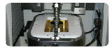
Dimension FastScan™ AFM has automatic imaging ability for big samples, making it widely used in the manufacturing process of the semiconductor and data storage equipments, it can measure diameter of 200 mm measured on more than 100 samples of the area. It has all the configuration of an atomic force microscope and the scanning tunneling microscope, can be used as surface roughness measurement defects detecting and other characteristics in the three dimensional and no damage to sample during the measurement process and don't need to sample pretreatment and modified.
(1)
Scanning Capacitance Microscopy (SCM)
Mainly use the change of majority carriers (electronic or electric hole) in samples (usually semiconductor) surface to imaging, apply an alternate voltage between the tip and sample, tip scan in surface samples, monitoring the capacitance change between tip and sample through a high sensitivity, high frequency oscillation circuit. SCM common used in semiconductor process analysis of 2D doping quantity distribution and defects.
(2)
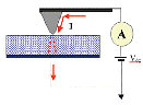
Conductive AFM (C-AFM)
Mainly used for analysis of the change of the semiconductor conductive of middle and low conductive semiconductors. For general use measurement. CAFM makes its current range fA to mA, and use conductive probe, in general operating under dc bias is applied by the point of a sample to let grounding. When using the z back to signal to produce award contact AFM image, the current will flow tip and samples, in order to produce the conductivity of the AFM image.
(3)
Scanning Spreading Resistance Microscopy (SSRM)
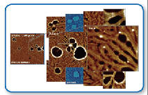
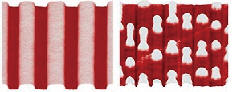
The patented Scanning Spreading Resistance Microscopy (SSRM) is the second kind instrument derived from Contact mode AFM, mainly used as imaging of a semiconductor materials 2D carrier concentration distribution (Resistance). When applied DC bias between tip and samples, and at the same time a conductive probe scan sample by contact mode, meanwhile, measure the current between tip and samples with 10pA to 0.1mA logarithm of current amplifier.
The right picture is SSRM image of the InP hetro-junction, the left picture is the Contact mode AFM (scan area is 7mm), pictures provide by Lucent Technologies. The different area of the hetro-junction of InP is clearly shown in the SSRM image:Zn-doped p type layer and S-doped n type area.
(4)
Surface Potential
Surface Potential (SP) imaging, is the second imaging mode derived from Tapping Mode, use the surface potential to image. When the tip under Lift mode (see "magnetic force microscope" in the description of the Lift Mode) scans through the samples above the surface, because each position potential is different between the tip and the surface of the sample, so there would be a force between cantilever and the tip. By transforming the voltage on the tip to make the tip and sample surface potential maintain consistent to offset force. SP images are used to detect and determine the difference of contact potential (CPD)
The right is CD RW Tapping mode measured figure and left for Surface Potential image, only in the Surface Potential images can present a bit (5µm scan range) Yasudo Ichikawa, Toyo Corp.
ContourGT Surface Measurement Systems - Non-contact Optical Profiler for QC/QA and research
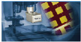
ContourGT™ series products combine with advanced bits, multi core operation and analysis software, patented white light of the interferometers (WLI) hardware, and easiest operation, is the most advanced developed 3D optical surface profile currently. Its designed is aim to have more advanced ability and higher productivity, strengthen current NT series which are mainly of WLI surface profile instrument. ContourGT series product contain a flagship level ContourGT-X, improver ContourGT-I and entry-level desktop K, Each product can offer all kinds of application of processing and manufacturing on the market (including high brightness LED, solar, ophthalmology, semiconductor and medical device, etc.).
ContourGT-K0
ContourGT-I
ContourGT-X
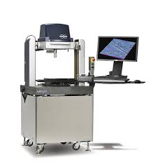
NPFLEX
Bump Ball height and Roundness measurement
Wired Die
Copper Wire imprint Depth and Aluminum Splash measurement
Laser Marking Depth Measurement
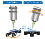
Traditional pitch-and roll stage designs require operator adjustment of five aces of motion to maintain point of inspection on line of sight for measurement. The unique Bruker tip/tilt in the head design maintains the line of sight on the point of inspection - regardless of tilt - resulting in optimized image acquisition and fastest time to data.
Equip with AFM module to further enhance the spatial resolution
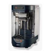
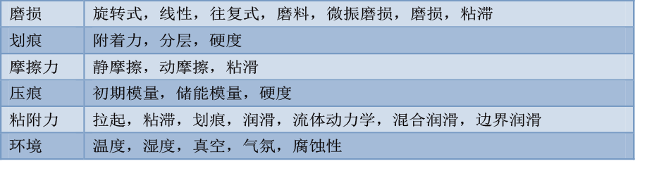
Universal Mechanical Testing (UMT)
By simply replacing components, within a matter of minutes users can alternate between reciprocating and rotating motion, from pin-on-disk to block-on-ring or any of a number of ASTM, DIN or ISO standard tests. Unlike other instruments in this class, Bruker's CETR-UMT is capable of highly accurate loading and custom motion patterns through the use of precision servo-control.
Disk / Disk Module
Disk / Disk Module
with 1000°C chamber
reciprocating Module
with 300°C chamber
Nanoindentation Module
* UMT-1 nano- & micro-mechanical tests of thin and ultra-thin coatings and bulk materials,
load range: 1µN - 10N
* UMT-2 micro-mechanical tests of coatings and materials, load range: 1mN to 200N
* UMT-3 macro-mechanical tests of lubricants, metal and ceramic materials, load range: 0.1N to 1kN
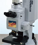
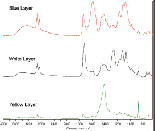
FTIR (Fourier transform infrared spectroscopy)
- using infrared spectroscopy and fourier transform to analyze contamination for process control and failure analysis
Specifications:
1. Resolution: 0.5cm -1,optional 0.25cm -1
2. SNR better than 40000:1 (1-min test)
3. Patented ROCKSOLID Interferometry, vibration-free
and maintenance-free
4. Can equip on IR microscope
5. Far IR Mid IR, near IR measurement
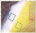
Using IR Microscope to define the
Region-Of-intest of the samples


.jpg)