Categories
Video


Teltec Pacific is a technical Sales and Service organisation serving the Semiconductor, Photonics and Optoelectronics Industries in Asia Pacific countries.

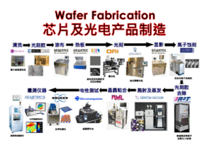
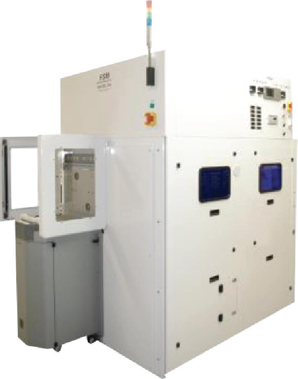
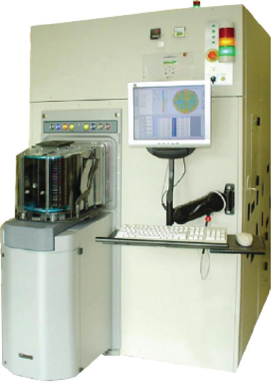
FSM - INLINE & DIMENSIONAL METROLOGY


FSM USA
INLINE & DIMENSIONAL METROLOGY


INLINE METROLOGY

Frontier Semiconductor (FSM) pioneered and commercialized the proprietary LASER OPTICAL LEVER (Optilever) technique now widely used in Film Stress and Wafer Bow Measurements.


FSM 900 SERIES

New materials are very sensitive to oxidation at elevated temperatures.  They are also prone to outgas or exhibit physical and material changes, the FSM 900TC-Vac offers a sealed heating type chamber that simulates process conditions. It can operate either under a completely inert gas environment (with very low partial pressure of oxygen) or under high vacuum mode.

• Characterization of Low K, Copper and other thin film materials
• Temperature up to 900
• Operation in vacuum or inert gas


FSM 128 SERIES

The FSM 128 Series is a Film Stress and Wafer Bow Measurement System.

• 128NT: Up to 200mm wafer
• 128L: Up to 300mm wafer
• 128G: Up to 450 mm wafer
• 128 C2C: Cassette to Cassette Fully Automated System up to 200mm wafer
• 128L C2C: Cassette to Cassette Fully Automated System up to 300mm wafer

All FSM 128 tools can be equipped with automatic Average Substrate
Thickness Measurement capabilities to evaluate the incoming wafers
used for stress evaluations.


DIMENSIONAL METROLOGY

Nondestructive optical probes from FSM addressing wafer thickness, TSV, bump and other dimensional Metrology needs.


FSM 8108 VITE SERIES

• Wafer Thickness, Membrane Thickness and TTV
• Absolute Thickness, Topography, Warp,
• Si, GaAs, etc.
• Tape, Glass, Sapphire, etc.
• Stacks of Multiple Materials
• Through Silicon Via (TSV) and Trench Depth with Microscope Option
• Bump Height Measurement
• Very Fast Measurements
• Optional Roughness Measurement for Back grind, Etched, Polished wafers
• Optional thin film measurement


FSM 413 SERIES

• Measures Substrate Thickness in Multiple Layers using Non-contact Optical System
• High Precision XY Stage (0.5 µm)
• Robotic Handling System
• Pogrammable Data Points
• Lateral Data
• TSV and Bump
• Measures Silicon via Depth with Microscope option
• Excellent Repeatability & Reproducibility
• Pattern Recognition Function


FSM RAMAN ADVANTAGES

Technology Innovation and Tool Automation

• Technology Innovations Leading to Compact System
• Superior performance in terms of spectral resolution (0.1 cm-1),
for device analysis
• Several years successful track record in wafer fab tool automation
and control in metrology (since 1988)