Categories
Video


Teltec Pacific is a technical Sales and Service organisation serving the Semiconductor, Photonics and Optoelectronics Industries in Asia Pacific countries.

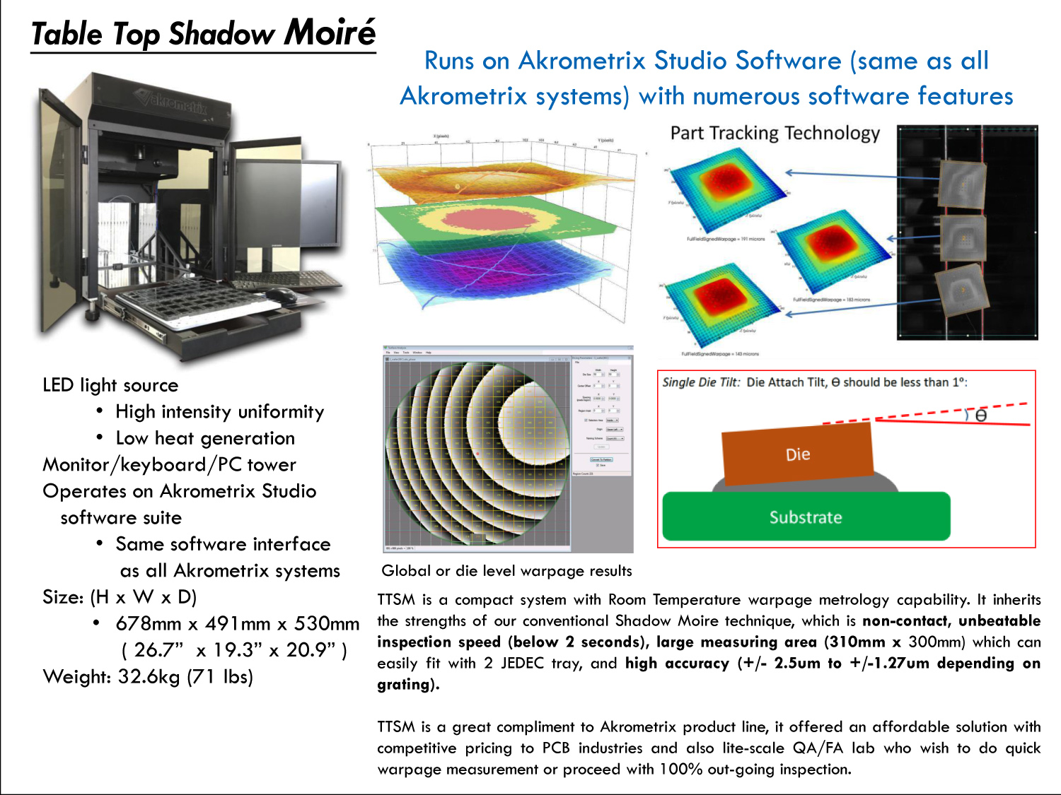
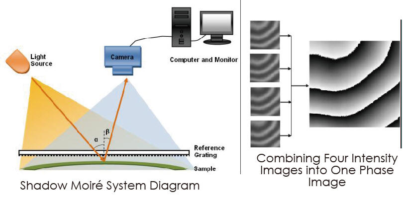
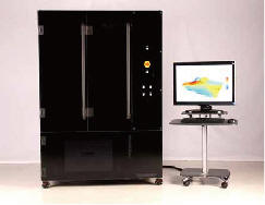
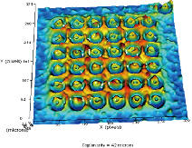
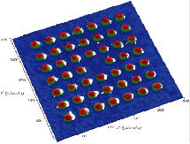
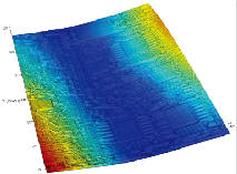
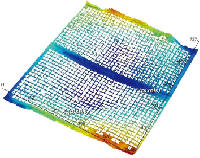
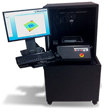
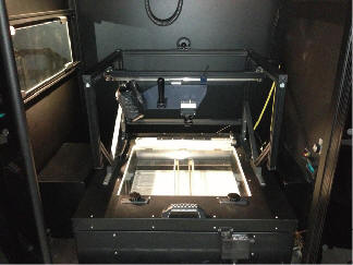
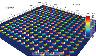
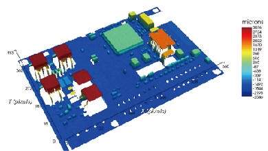
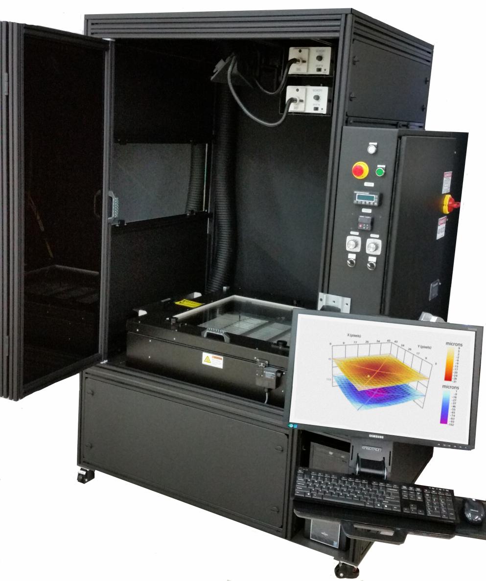
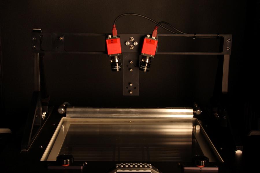
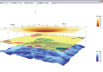
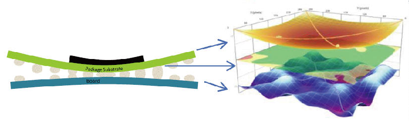
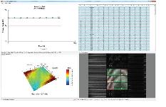
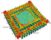
Akrometrix - Automated Flatness Inspection

Akrometrix, USA
 

Automated Flatness Inspections Systems
Akrometrix is the leading provider of full-field modular metrology solutions for substrates and packages in the OEM, CEM, SATS and PCB segments of the global microelectronics industry. Akrometrix's TherMoiré and LineMoiré product lines offer comprehensive flatness characterization capabilities for development and production applications. A pioneer in the temperature dependent measurement arena, Akrometrix's solutions are utilized by 95% of the top 20 global semiconductor manufacturers.

The new generation of surface measurement and analysis techniques

Development/Diagnostics /Production Monitoring. Whether your customer is the individual consumer or an OEM, the TherMoiré excels at helping you achieve exceptional customer satisfaction. Better than ever, TherMoiré technology can simulate your thermal processing and operating environment conditions, while capturing a complete history of out-of-plane displacement behavior. Applying this critical information to form - or achieve compliance for - component/substrate behavior allowances (i.e. warpage specifications) can directly impact level I & level II assembly yields and enhance product reliability. Below data could be measured: Coplanarity, Sign warpage, Fulfill warpage, Twist, Bow, CTE, etc.


Press Release:

  • Advanced Second Level Assembly Analysis Techniques - Ken Chiavone's Global SMT & Packaging Article 

  • NEW!!! Press Release (Jan-20-2014) - The CXP for Cost-effective Elevated Temperature Surface CharacterizationTM 

  • NEW!!! Press Release (Jan-16-2014) - The Convection Reflo Emulation Module (CRE) for Next Generation Reflow Emulation Combined with Surface CharacterizationTM 


Product Applications:

  • Introduction to High Volume Testing Protocol with Part TrackingTM  / Applications

  • High Volume Testing Protocol/Best Practices  / Applications 

  • Die and Package Testing Protocol/Best Practices  / Applications

  • PCB Testing Protocol/Best Practices  / Applications

  • Socket Testing Protocol Summary  / Applications


NEW !!

Table Top Shadow Moiré (TTSM)
For fast, room temperature warpage metrology


Shadow Moiré Technology

Shadow Moiré is a non-contact, full-field optical technique that uses geometric interference between a reference grating and its shadow on a sample to measure relative vertical displacement at each pixel position in the resulting image. It requires a Ronchi-ruled grating, a white line light source at approximately 45 degrees to the grating and a camera perpendicular to the grating. Its optical configuration integrated with the heating chamber is shown in the figure below. A technique, known as phase stepping, is applied to shadow moiré to increase measurement resolution and provide automatic ordering of the interference fringes. This technique is implemented by vertically translating the sample relative to the grating.

Thermal Shadow Moire to Cross-section Correlation Study


TherMoiré AXP Features
  • Max measure area 400mm x 400mm

  • Dynamic Temperature Profilling-temperature range from -55°C  to 300°C

  • Support the simulation of the reflow oven temperature from  room temperature to 300°C

  • Maximum heat 2 degrees Celsius per second

  • Modular Metrology - Shadow Moiré, Digital Image Correlation,    Micro Fringe Projection

  • Automated Analyses - Bow, Twist, Coplanarity, Chamber, CTE,     Surface Tilt, etc

  • Data Management - Centralized database tools for production     monitoring, trending and customer conformity/assurance     requirements.

  • Support multi-sample test at the same time, increase production


For small samples can also measure warpage

PCB

Socket

QFN (3mm x 3mm)


Digital Fringe Projection - DFP Module
  • Enables step height and discontinuous surface measurement

  • FOV can be moved to anywhere on the sample (gantry fixture)

  • Improved top/bottom temperature uniformity – no grating

  • High X/Y resolution for solder ball coplanarity measurement

  • Maximum FOV – 48mm x 64mm

  • Maximum Sample Size – 300mm x 300mm

  • Minimum Sample Size - .5mm x .5mm

  • Resolution, Z-axis – 5 microns

  • Accuracy, Z-axis – 5 microns


CXP Projector/Camera Gantry BGA Solder Ball Measurement

Enables step height and discontinuous
surface measurement


FOWLP Panel Warpage Metrology System - AKM600P FOWLP
The Akrometrix AKM600P is a warpage metrology solution
  • Specifically designed for the FOWLP market

  • Utilizes shadow moiré to measure warpage, down to 1.25µm in z-resolution
  • Full Field of View, Single Shot metrology in less than 2 seconds
  • Able to accommodate panels up to 600mm x 600mm
  • Can also accommodate wafers - perfect bridge tool
  • Optional oven to measure warpage in temperatures ranging from 26°C to 300°C


Fan Out Wafer Level Processing (FOWLP)


Digital Image Correlation - DIC (2.0) Module
  • Add-on Module to: AXP & PS200S

  • Strain and CTE measurement module

  • Data acquisition time < 1 second

  • In-Plane Resolution: < 1.0 μm

  • Strain Resolution: < 150 microstrain (Δ L/L x 10-6)

  • Temperature Range: 26°C to 300°C

  • Field of Views: 75 mm x 75 mm

DIC 2.0 Module installed

in the TherMoiré AXP

Strain measurement can be critical for components, PBCs, and material layers

Mean strain values used

for CTE calculation


Akrometrix Studio 8.3.2 Software

Akrometrix Studio is an advanced set of integrated software modules that work together to provide the most comprehensive set of surface characterization and analysis capabilities available. When used with the TherMoiré AXP surface measurement system, Studio powers a set of modular metrology solutions that generate fast, comprehensive surface information characterizing a wide range of microelectronic components and assemblies. Studio enables the user to draw conclusions and make decisions using a variety of powerful graphical and analytical analyses.


Interface Analysis Software

Trouble Shooting & Assembly Defects?

* HNP/H0P
* SHORTS
* OPENS

3D graphical analysis of the gap between
components during the reflow process 
Pass/Warning/Fail Maps


AXP POP Module (Convection Add-on Module)

Combines maximum resolution capabilities of the AXP with the ability to measure discontinuous surfaces

  • Convection heating and cooling

  • Temperature uniformity consistent with Production/Assembly    convection reflow ovens

  • Submicron resolution capabilities/ multi-part testing

  • Field of View (FOV) – 75mm Circle


POP Module


Studio Software Real-time Analysis Release
Combines High Volume Testing with Go/No Go Criteria
  • Enables user-defined ‘Pass/Fail’ limits applied to measurement results

  • Visual Pass/Fail indicators immediately after measurement

  • Works with Part Tracking for Multiple Part Testing

  • Works at Room Temperature and During Thermal Profile